Cool Power, Inside and Out |
| |
|
 |
GIGABYTE Ultra Durable™ 5 motherboards use IR3550 PowIRstage® ICs, which feature the industry's highest 60A rating, with Lower Losses, Higher Efficiency and Excellent Thermal Management.
|
|
 |
The layout and packaging use copper connections for all power paths rather than wire bonds, reducing losses due to high resistance wire bonds as well as high inductance which causes ringing and high AC losses.
|
Power connections between the MOSFETs use very low loss copper, reducing losses and helping to spread the heat. |
Specialized MOSFET driver IC by International Rectifier. |
High side MOSFET (Control FET) has very low gate charge. Low side MOSFET (SyncFET) has an integrated Schottky Diode for even higher efficiency. |
The current has very short paths from the bottom of the device, through either the control FET (duty cycle ON) or the Sync FET (Duty cycle OFF) and through the copper clip. This is another reason the device is so durable and can handle 60A. |
Custom Copper leadframe conducts heat away from the silicon. |
|
|
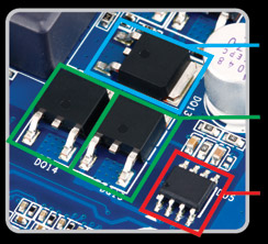
Traditional CPU Power Zone Design |
PWM controller |
MOSFET Drivers |
Traditional High and
Low side MOSFETs |
Choke |
Capacitor |
CPU |
|
| |
CPU Power Zone Q & A
|
| |
What is the CPU Power Zone ?
The CPU Power Zone contains the various components of a motherboard that are responsible for delivering power to the CPU (PWM controller, MOSFET Drivers, High and Low side MOSFETs , Chokes, Capacitors and related circuitry).
What is a MOSFET ?
A MOSFET is one of the most critical components of the CPU power zone, as it is a switch that first allows or disallows electric current to flow to the CPU. Its switching is controlled by the MOSFET driver and PWM controller. It is also one of the most expensive components of the power design.
What is a Power Stage ?
A Power Stage is a single chip that includes the MOSFET driver, 1 high side MOSFET and 2 (or sometimes 1) Low Side MOSFETs . Power Stages are made using a more advanced manufacturing process, and are therefore more efficient.
What is a Traditional MOSFET (Also known as D-Pak MOSFET...) ?
A Traditional MOSFET is a less advanced MOSFET design that is used in a traditional CPU power zone where the MOSFET drivers and High and Low Side MOSFETS are each individual chips (multi-chip MOSFET design). They are less expensive and less efficient than single chip Power Stages. |
|
|
| |
| |
| |
| |
|
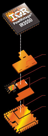
IR has leveraged it's world class packaging technology developed for the DirectFET®, improving the thermal capability and layout of the PowIRstage® significantly over that of other MCM packages.
|
| |
Single Package Design* |
vs. |
|
|
| |
Driver IC |
| |
|
* patent pending |
|
|
|
Other MOSFET layout implementations use a multi-chip, side-by-side arrangement of the high and low side MOSFETs and driver IC, taking up significant board real estate and creating more electrical leakage. |
 |
High Side MOSFET
(Traditional MOSFET) |
| |
Low Side MOSFET
(Traditional MOSFET) |
| |
Driver IC
(MOSFET Driver) |
|
| |
|
|
| |
|
|
| |
| |
| |
| |
|
Power Stage
(Also known as IR3550
PowIRstage® ) |
Lower RDS(on) MOSFET (Ultra Durabnle™ 4 Design)
(Also known as WPAK, PowerPAK MOSFET...) |
|
|
Traditional MOSFET (Also known as D-Pak MOSFET...) |
|
| |
Size ratio between objects is constant |
|
|
|
| |
| |
| |
| |
Driver IC Developed by International Rectifier |
IR3550 PowIRstage® ICs feature a specialized MOSFET driver IC which is tuned perfectly for the MOSFET pair. Many Driver MOSFET companies use drivers from other companies, thus the drivers are not really optimized for the MOSFETs. With co-packaged Driver+MOSFETs, IR has designed this driver to optimize this module for greatest efficiency. |
| |
|
|
 |
|
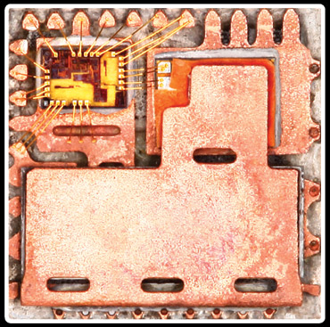
IR3550 Power Stage X-ray picture |
|
IR3550 Power Stage decapsulation picture |
|
|
| |
| |
| |
Ultra Cool, Ultra Efficient, Ultra Performance |
High Efficiency = Low Power Loss = Less heat = Longer Lifespan |
| |
| |
IR's IR3550 PowIRstage® are more power efficient and operate cooler than competing MOSFETs, resulting in longer component lifespan and more head room for greater overclocking performance.
|
| |
Traditional MOSFET
|
IR3550 PowIRstage®
|
|
|
|
|
| |
|
|
|
* Testing result for reference only. Results may differ according to system configuration.
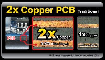
* 4 phase IR3550 PowIRstage® with 2x Copper PCB vs. 4 phase traditional MOSFET @ 100A load 10 mins lab testing without heatsink. |
| |
| |
| |
IR3550 PowIRstage® ICs feature greater power efficiency and are the industry's highest rated MOSFETs, able to provide up to 60A of power. This ensures the best power delivery to the CPU, for more stable operation and better overclocking performance. |
| |
16 Traditional MOSFETs
in Operation
|
4 PowIRstage® ICs in Operation |
|
|
|
|
|
| |
 |
| |
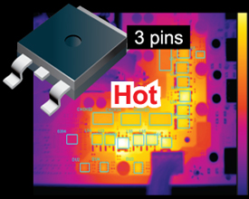
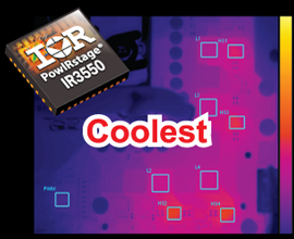
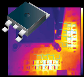
IR3550 PowIRstage® ICs are so efficient, that even though the 4 PowIRstage® ICs in operation on the right are doing the same workload as the 16 traditional MOSFETs in operation on the left, their temperature is still up to 30° C cooler than the traditional MOSFET design. |
|
|
|
|
| |
* Testing result for reference only. Results may differ according to system configuration.
Configuration: Intel Core™ i7-3770K CPU, Default CPU frequency (3.5GHz), 1.2V Vcore, Default BIOS setting, DDR3 1333MHz, 500W PSU, CPU water cooling with no MOSFET heatsink. Software: Microsoft Windows® 7 running Power Thermal Utility at 100% loading. |
| |
IR3550 PowIRstage® ICs remain cooler than other MOSFET designs, allowing users to overclock to greater levels of performance. Each power component has a maximum thermal operational temperature, and once it is reached, adding more voltage will only result in a failed overclock. Since IR3550 PowIRstages® are able to operate at cooler temperatures at higher voltages than traditional designs, overclockers are able to have more headroom to increase voltages, resulting in higher potential overclocks. |
Cooler temps. = Higher Overclocks |
MOSFET Overclocking Stability |
|
Overheat |
Not enough power
for overclocking |
|
|
 |
IR3550
PowIRstage® |
Best |
|
 |
Lower RDS(on)
MOSFET
(Also known as WPAK, PowerPak MOSFET...) |
Good |
|
 |
Traditional MOSFET
(Also known as D-Pak MOSFET... ) |
OK |
| |
|
|
|
| |
| |
| |
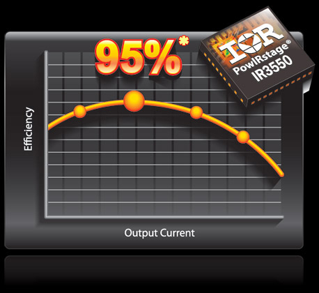
Industry Leading Peak Efficiency up to 95%* |
| |
 |
| |
IR3550 PowIRstage® ICs are more efficient, with peak efficiency up to 95%, during normal operation.
Even at higher Current levels, IR3550 PowIRstage® ICs are able to maintain lower power losses. Lower power loss also means less heat as a byproduct. |
| |
| |
| |
* Testing result for reference only. Results may differ according to system configuration.
VIN=12V, VOUT=1.2V, ƒSW = 300kHz, L=210nH (0.2mΩ), VCC=6.8V, CIN=47uF x 4, COUT =470uF x3, 400LFM airflow, no heat sink, 25°C ambient temperature, and 8-layer PCB of 3.7" (L) x 2.6" (W). |
| |
|
|
Current Typical MOSFET Designs
|
| |
|
|
|
|
| |
Power Stage
(Also known as IR3550 PowIRstage®) |
Premium Cost |
|
Highest Efficiency
Lowest Temperature |
| |
Lower RDS(on) MOSFET
(Also known as WPAK, PowerPAK,
MOSFET...) |
High Cost |
|
Good Efficiency
Low Temperature |
| |
Traditional MOSFET
(Also known as D-Pak MOSFET...) |
Low Cost |
|
Low Efficiency
High Temperature |
|
|
| |
|
|
| |