View complete spec list
Graphics Card Comparison
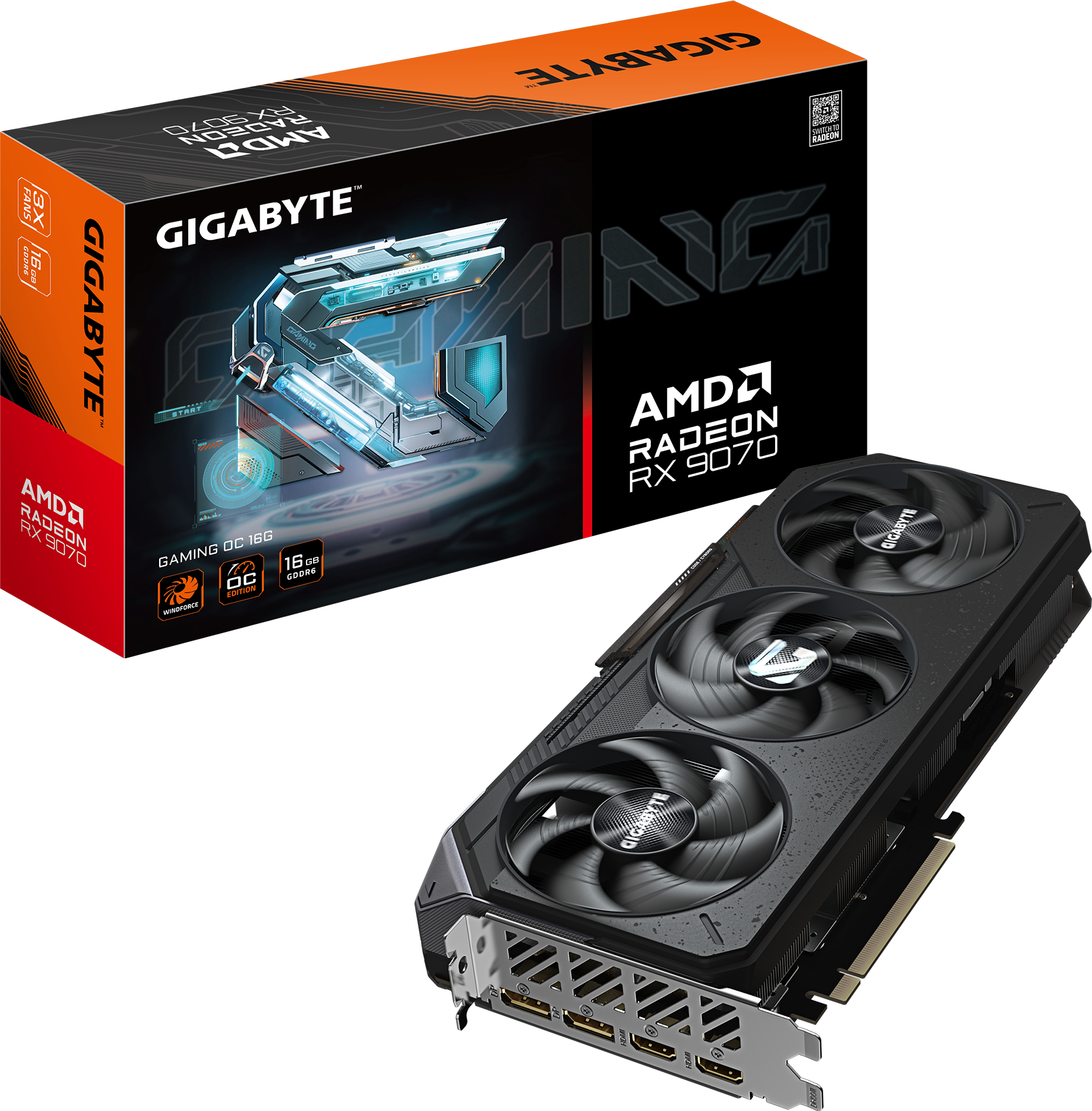
Radeon™ RX 9070 GAMING OC 16G
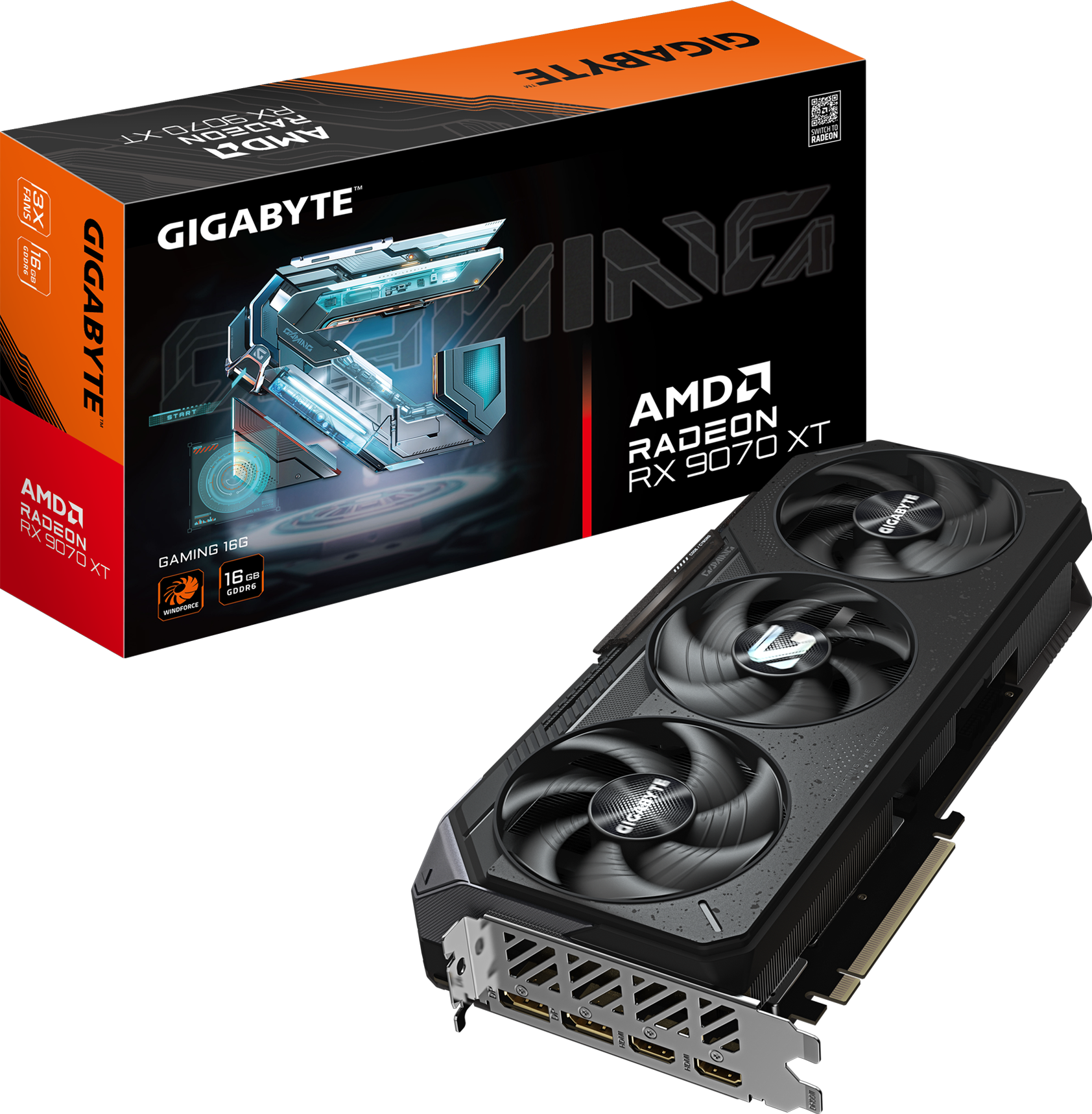
Radeon™ RX 9070 XT GAMING 16G
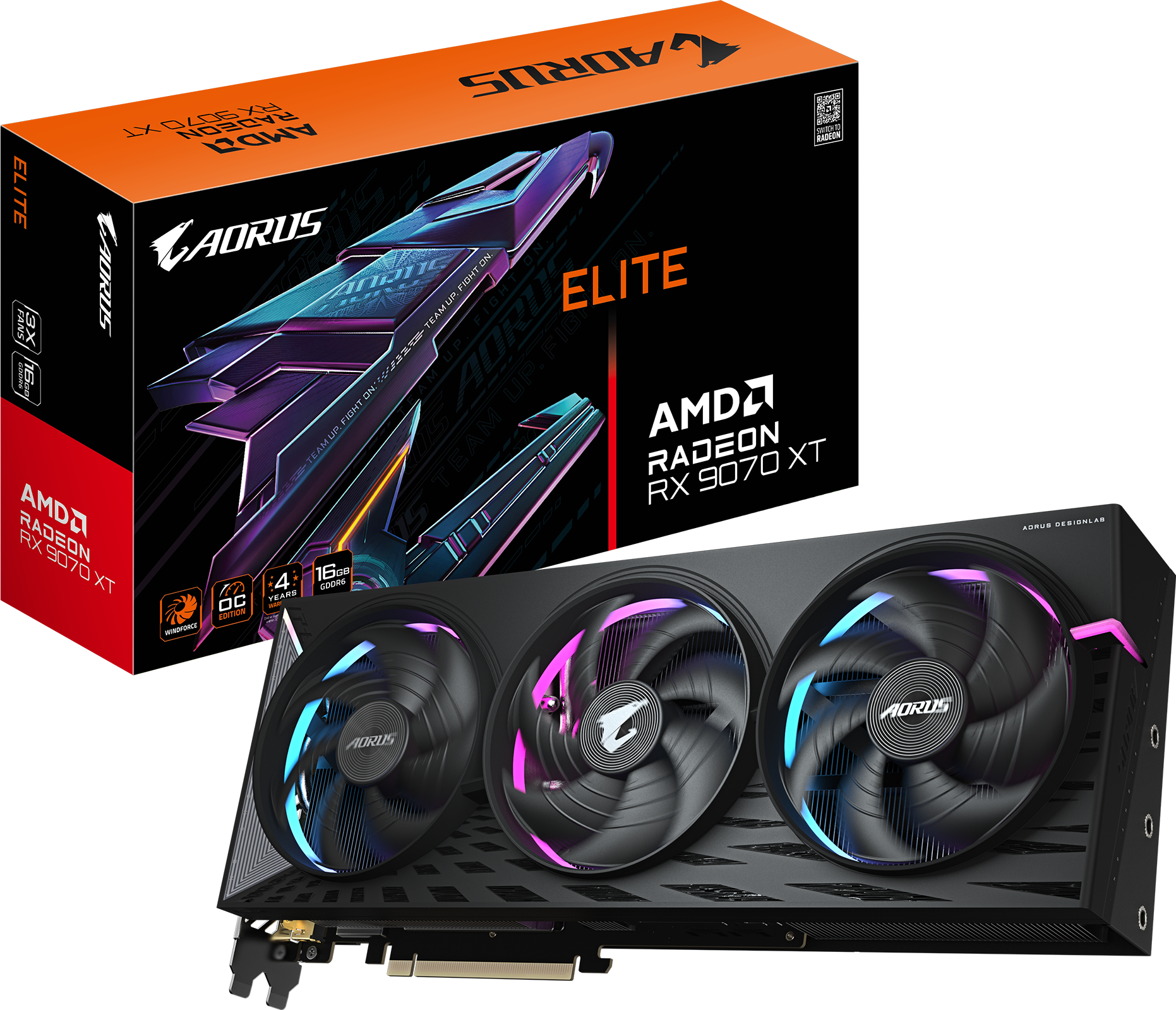
AORUS Radeon™ RX 9070 XT ELITE 16G
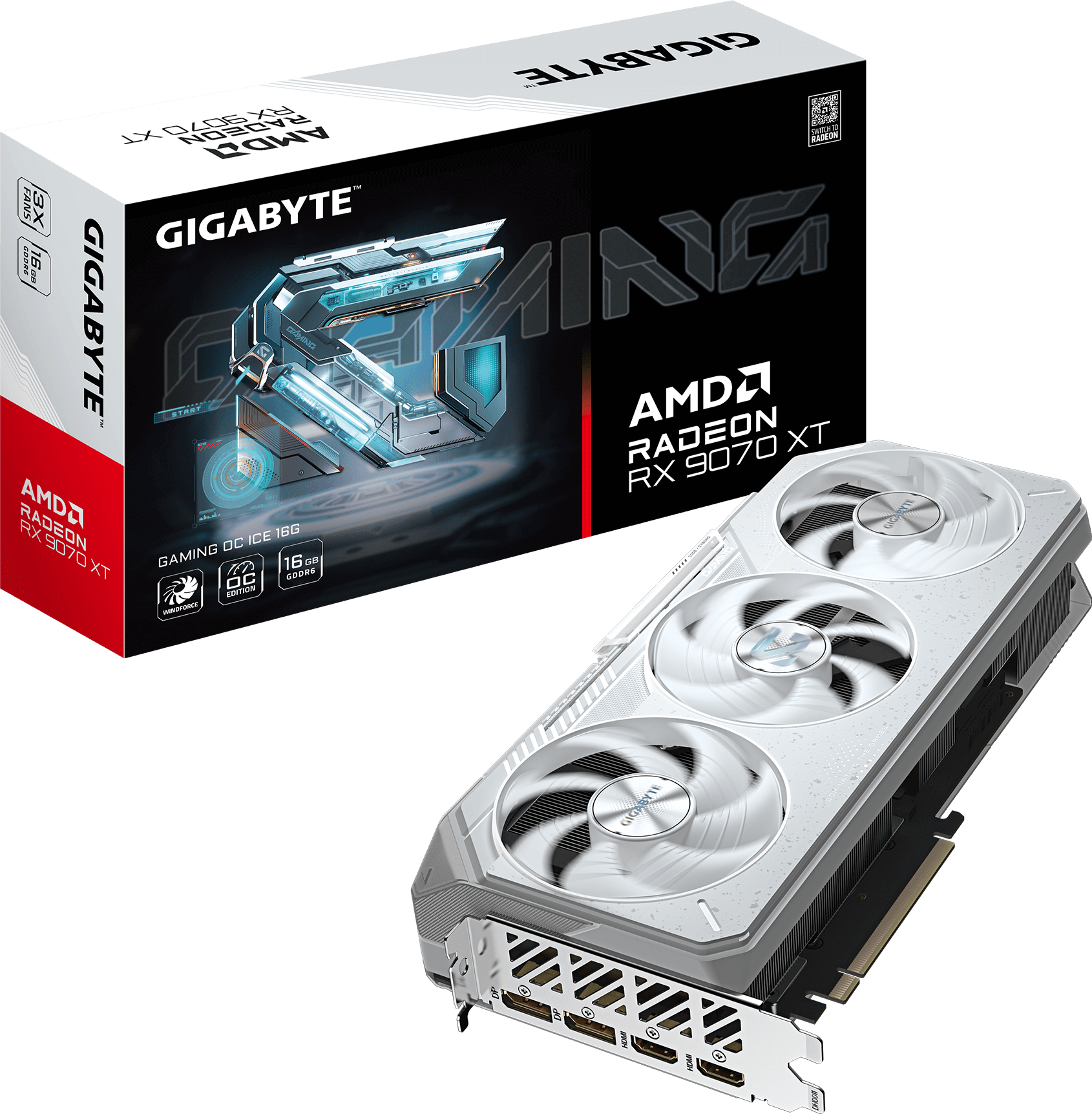
Radeon™ RX 9070 XT GAMING OC ICE 16G
- Quick Navigate
- Graphics Processing
Graphics Processing
Radeon RX 9070Radeon™ RX 9070 XTRadeon™ RX 9070 XTRadeon™ RX 9070 XT- Core Clock
Core Clock
Boost Clock* : up to 2700 MHz (Reference card: 2520 MHz)
Game Clock* : up to 2210 MHz (Reference card: 2070 MHz)Boost Clock* : up to 2970 MHz
Game Clock* : up to 2400 MHzBoost Clock* : up to 3100 MHz (Reference card: 2970 MHz)
Game Clock* : up to 2570 MHz (Reference card: 2400 MHz)Boost Clock* : up to 3060 MHz (Reference card: 2970 MHz)
Game Clock* : up to 2520 MHz (Reference card: 2400 MHz)- Stream Processors
Stream Processors
3584 ( 56CU)409640964096- Memory Clock
Memory Clock
20 Gbps20 Gbps20 Gbps20 Gbps- Memory Size
Memory Size
16GB16GB16GB16GB- Memory Type
Memory Type
GDDR6GDDR6GDDR6GDDR6- Memory Bus
Memory Bus
256 bit256 bit256 bit256 bit- Card Bus
Card Bus
PCI-E 5.0PCI-E 5.0PCI-E 5.0PCI-E 5.0- Digital max resolution
Digital max resolution
7680 x 43207680x43207680x43207680x4320- Multi-view
Multi-view
4444- Card size
Card size
L=288 W=132 H=50 mmL=288 W=132 H=56 mmL=339 W=136 H=59 mmL=288 W=132 H=56 mm- PCB Form
PCB Form
ATXATXATXATX- DirectX
DirectX
DirectX 12 APIDirectX 12 APIDirectX 12 APIDirectX 12 API- OpenGL
OpenGL
OpenGL 4.64.64.64.6- Recommended PSU
Recommended PSU
750W850W850W850W- Power Connectors
Power Connectors
8 pin*28 pin*38 pin*38 pin*3- Output
Output
DisplayPort 2.1a x2
HDMI 2.1b x2DisplayPort 2.1a *2
HDMI 2.1b *2DisplayPort 2.1a *2
HDMI 2.1b *2DisplayPort 2.1a *2
HDMI 2.1b *2- Accessories
Accessories
VGA manualQuick guide1. Quick guide
2. Warranty registration
3. AORUS metal sticker
4. Versatile VGA holder
5. Versatile VGA holder manualQuick guide- Note
Note
* “Boost Clock” is the maximum frequency achievable on the GPU running a bursty workload. Boost clock achievability, frequency, and sustainability will vary based on several factors, including but not limited to: thermal conditions and variation in applications and workloads. GD-151
* “Game Clock” is the expected GPU clock when running typical gaming applications, set to typical TGP (Total Graphics Power). Actual individual game clock results may vary. GD-147* “Boost Clock” is the maximum frequency achievable on the GPU running a bursty workload. Boost clock achievability, frequency, and sustainability will vary based on several factors, including but not limited to: thermal conditions and variation in applications and workloads. GD-151
* “Game Clock” is the expected GPU clock when running typical gaming applications, set to typical TGP (Total Graphics Power). Actual individual game clock results may vary. GD-147* “Boost Clock” is the maximum frequency achievable on the GPU running a bursty workload. Boost clock achievability, frequency, and sustainability will vary based on several factors, including but not limited to: thermal conditions and variation in applications and workloads. GD-151
* “Game Clock” is the expected GPU clock when running typical gaming applications, set to typical TGP (Total Graphics Power). Actual individual game clock results may vary. GD-147


